Report Period: 12/1/2000 to 4/2/2001
URL for this report: http://www.cse.psu.edu/~chip/pdg/rp1/report1.html
Report Slides(.ppt): http://www.cse.psu.edu/~chip/pdg/rp1/report1.ppt
1. Summary of the Quarterly Technical Report 1
2. Design Method
Systematic variation approach
CAD tools
experimental base, spice model base
3. Chip Layout Design
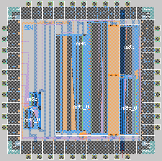
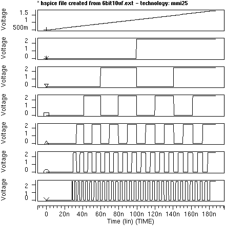
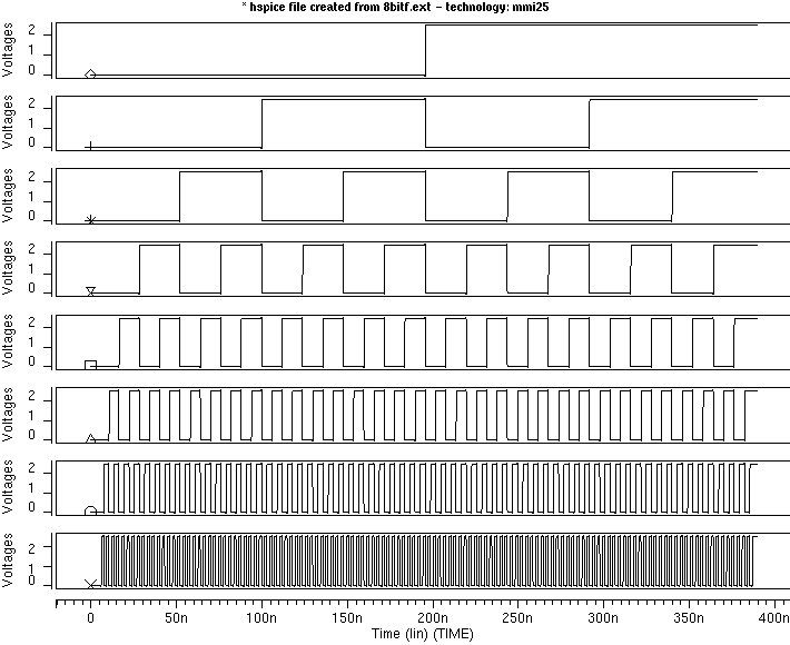
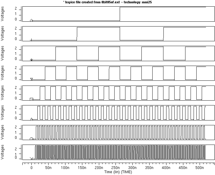
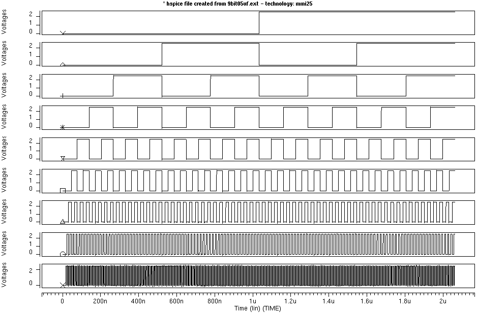
ADC Sizes and Layouts
Pad Size and Layout
Multiplexor Size and Layout
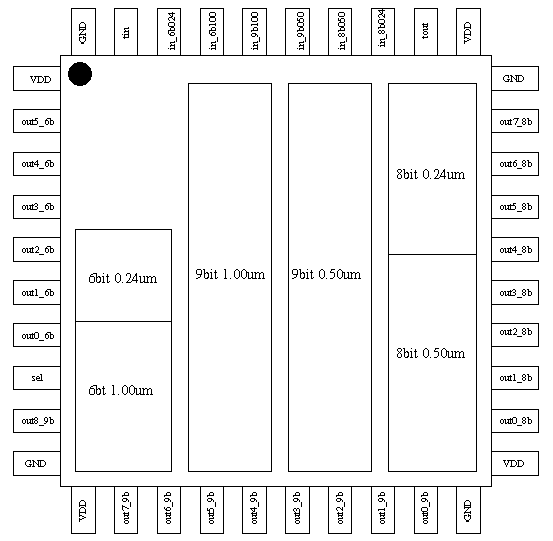
Chip Block Diagram
4. Simulation Results
Speed and Power Consumption of ADCs
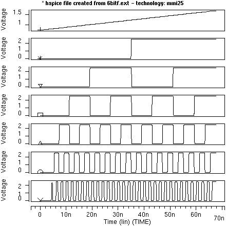
INL, DNL
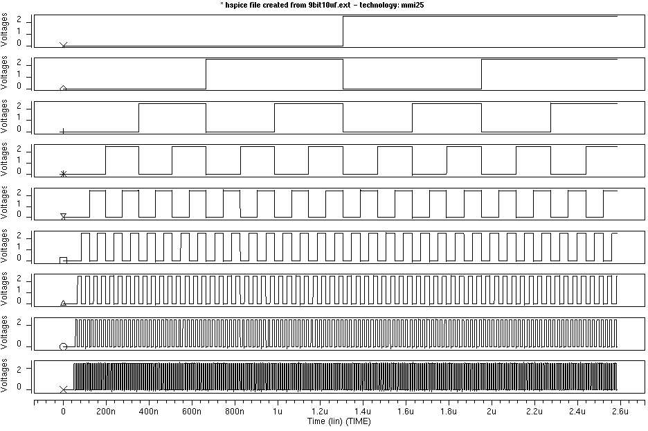
Sampled sine wave spectrum
Process variation
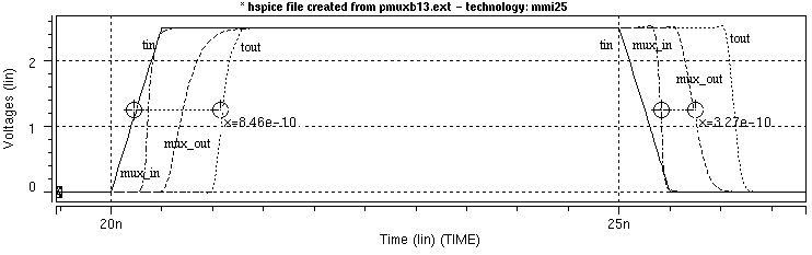
Delay of Pad and Multiplexor
5. Fabrication Submission
6. Evaluation/Future Work/Conclusion
Features of the TIQ based ADC
Issues to be addressed in future
Appendix
Program sources
Presentation Slides
Schematics of 3bit TIQ based ADC
PROJECT GOALS FOR THIS QUARTER
(1) Design a 6 and 8 bit TIQ based flash ADC circuits and CMOS layout
(2) Design the first prototype chip: 6 and 8 bit flash ADC
(3) Chip fabrication submission
ACCOMPLISHED PROJECT MILESTONES FOR THIS QUARTER
(1) Designed a 6, 8, and 9 bit TIQ based flash ADC circuits and CMOS layout in 0.25 um technology
a. Total six ADCs are designed:
i. a 6bit high speed ADC
ii. a 6bit low power ADC
iii. an 8bit high speed ADC
iv. an 8bit low power ADC
v. a 9bit high speed ADC
vi. a 9bit low power ADC
b. Circuit design, layout design, simulation, verification, and synthesis
c. TIQ comparator section design and thermometer code-to-binary code encoder design
d. TIQ comparator layout generator program design
e. ADC power optimization
(2) Designed the first prototype chip: 6, 8, and 9 bit flash ADC
a. Custom pad-frame design
b. Floor-plan design and place \& route 6, 8, and 9 bit ADCs (total six ADCs)
c. Chip design simulation, verification, and synthesis
(3) Fabrication submission preparation
(4) Chip fabrication submission
a. Submission date: 4/2/2001
b. Vendor: MOSIS with TSMC 0.25 um foundry
c. Expected prototype chip delivery date: 7/16/2001
FACULTY AND STUDENTS SUPPORTED
(1) Principal Investigator: Kyusun Choi, Assistant Professor, Department of Computer Science and Engineering
(2) Graduate Assistant 1: Jincheol Yoo, Ph.D. student, Department of Computer Science and Engineering
(3) Graduate Assistant 2: Daegyu Lee, MS student, Department of Computer Science and Engineering
PUBLICATION
Paper Accepted (during this quarter) to Appear: J. Yoo, K. Choi, and A. Tangel, A 1-GSPS CMOS Flash Analog-to-Digital Converter for System-on-Chip Applications, the IEEE Computer Society Workshop on VLSI.
(1) Designed a 6, 8, and 9 bit TIQ based flash ADC circuits and CMOS layout in 0.25 um technology
a. Total six ADCs are designed:
i. a 6bit high speed ADC
ii. a 6bit low power ADC
iii. an 8bit high speed ADC
iv. an 8bit low power ADC
v. a 9bit high speed ADC
vi. a 9bit low power ADC
b. Circuit design, layout design, simulation, verification, and synthesis
c. TIQ comparator section design and thermometer code-to-binary code encoder design
d. TIQ comparator layout generator program design
e. ADC power optimization
(2) Designed the first prototype chip: 6, 8, and 9 bit flash ADC
a. Custom pad-frame design
b. Floor-plan design and place \& route 6, 8, and 9 bit ADCs (total six ADCs)
- Pad
Size(W*H): 2580 um * 2580 um
Layout
- Multiplexor
Size(W*H): 15.450 um * 14.530 um
Layout
Chip Block Diagram
(2) Chip fabrication submission
a. Submission date: 4/2/2001
b. Vendor: MOSIS with TSMC 0.25 um foundry
c. Expected prototype chip delivery date: 7/16/2001
d. GDSII file (45MB, use "Save as" to download the file)
(3) Project Status:
a. Design number 62265 status is QUEUED FOR FAB
b. Design name is "chip4"
c. Technology is TSMC25.
d. Fabrication restricted to TSMC only.
e. This project can be fabricated on a TSMC_025SPPM run.
f. Layout format is GDS COMPRESSED.
g. Top or root structure is "chip4".
h. Layout file is complete; Binary CRC checksum is 2144600049, 134471442
i. Counted 40 bonding pads.
j. The layout size is 2580 x 2580 microns.
k. Layers found: CONTACT, METAL1, METAL2, METAL3, METAL4, METAL5,
N_PLUS_SELECT, N_WELL, PASSIVATION, POLY, P_PLUS_SELECT,
RPO, THIN_OXIDE, VIA, VIA2, VIA3, VIA4, VTD_N
l. Requested package is DIP40
m. Requested quantity is 25 (0 unpackaged)
n. You ordered a total of 25 parts
o. 25 to be packaged in DIP40
p. The charge for project fabrication will be $11350.00
(1) Features of the TIQ based ADC:
a. High-speed
b. Relatively small area
c. Relatively low-power
(2) Issues to be addressed in future:
a. Dynamic fine-tuning
b. Supply voltage variation compensation
c. Temperature variation compensation
d. Process variation compensation
e. Lower power
f. FIFO design for on-chip high-speed data acquisition
(1) Program sources
mkinv.c; making inverters of specified range of size
fndsizes.c; finding desirable sizes of inverter
buildcomp.c; building up a comparator part using selected inverter sizes in previous step.
(2) Presentation slides
Click here for the presentation slides (Power Point file).
(3) Schematics of 3bit TIQ based ADC
Click here for the schematics
Incorporated in 1995, Micro Magic, Inc. is the industry leader in true 3-dimensional TSV layout tools. Click here for the full story
Engineers from Micro Magic meet with your engineers and management, to discuss the best solution to the problem or problems in the chip design. Some issues are smaller, and more easily remedied; some are larger and will require more involvement. Micro Magic's intention is to provide the most efficient solution utilizing your current design flow and our development tools. Our engineers can either do the work off-site, in house, or provide the MMI tool(s) and advice for a plug-n-play augmentation to your existing flow.
Trying to achieve the performance we needed from commercially-available tools just wasn't working. Over the course of several years, Micro Magic's engineers wound up writing their own tools to help get chips out. Our design services history is unmatched for making tapeout on time. Of course, our clients began to notice that MMI engineers were more efficient, more productive, and started asking about the tools. We responded by making them available to other engineers,and in 1995 the first versions of MAX and SUE were ready for the public..
Micro Magic, Inc.
Sunnyvale, CA
408.414.7647 x202
info at micromagic.com.