by Lee Tavrow, John Johnson, and Mark Santoro
Traditional design flows don't efficiently support the implementation of large, regular structures in IC design. At Micro Magic, we've created a proprietary high-speed, low-power SRAM and implemented a supporting design flow based on currently available, standard analysis tools and three design tools we created. The design flow has been optimized to reduce the design time and guarantee correct behavior at first tape-out. Variable-size SRAMs can be automatically generated, and the design can be quickly retargeted to a different technology.
Micro Magic is a small, fabless semiconductor design company. Formed in January 1995 to design microprocessors under contract, we have since taken on other designs, including SRAMs. During the course of designing various chips, we built and refined three design tools so that we could implement a streamlined, error-reducing design flow. The design flow was further refined during the design of the SRAM.
Our SRAM is currently under patent review for some unique techniques that yield high speed--700 MHz using 0.25-µm technology-- low power, and high noise immunity. These characteristics are particularly valuable for embedded caches for microprocessors.
One of the primary goals during the design was to create a design flow that would allow us to quickly generate various-size SRAMs, depending on the design needs at the time. To do that, we had to employ a generator. We also needed to greatly reduce the verification time over the standard SRAM design flow so that when a new-size SRAM is generated, it can be completely verified quickly.
Another major goal of the design flow was to be able to switch technologies quickly. The design flow supports this capability through the use of a megacell generator and efficient verification techniques.
The design and layout of the SRAM was completed in 3 1\2 calendar months with approximately 9 person-months of effort. This period started from the receipt of the foundry six-transistor cell and technology rules and was completed with final tape-out. Under the same technology rules, we can generate and verify different sizes of the SRAM up to 32 kbytes with 16 to 128 outputs in less than 1 week. Furthermore, multiple copies of the 32-kbyte SRAM can be combined to create larger designs. Implementing the same design with different technology will require about 3 person-months of effort. The effort is split between verifying and optimizing the timing of the design and creating the layout. The generator doesn't have to be modified.
The traditional design flow Large, regular structures like SRAMs don't fit into current EDA design flows. The most common approach has been to create a small, representative schematic; generate or manually enter a schematic of the entire SRAM; lay out the entire SRAM by hand; functionally verify the design and then perform LVS; and extract a Spice netlist from the layout and perform critical path analysis.
A small representative schematic is used to refine the timing for the SRAM and is similar to the first step in our design flow. After that, the design flows diverge.
Generating a schematic of the entire SRAM has been necessary to perform LVS with the final layout. There's been no other way to verify that the layout performs as designed in the schematic. However, generating a full schematic is time-consuming and error-prone. Furthermore, these large schematics aren't compact and are hard to read and understand.
Because the layout is done by hand for the entire SRAM, generating a new-size SRAM in the same technology is still considerable hand work, and moving to a new technology requires a completely new layout.
As for verification, the process is unwieldy and time-consuming on several levels. Functional verification is done by running vectors on a netlist generated from the schematic and then performing LVS using the large, unwieldy schematic and the large, very regular layout. LVS of an SRAM is a difficult problem for available programs, because they frequently generate false errors, and much time is spent determining if the reported errors are real. In addition, the programs have problems reporting errors on large, repetitive structures; LVS therefore doesn't exhaustively test the functionality of the final layout, which would be the optimal method for determining if the design is correct.
Spice models are useful for critical path analysis, but they must be extracted by hand from the complete design--a tedious and error-prone procedure. Using the complete design for running Spice for timing analysis of the critical path isn't possible because the problem is too large. Fast Spice simulators such as ADM could be used, but the accuracy for timing analysis is reduced without gaining enough simulation speed to do exhaustive functional analysis.
What's more, the design flow creates many possibilities for errors to be introduced and not caught. Also, there is little flexibility for creating derivative designs quickly.
The new design flow The goals of our design flow were to eliminate these problems. To do that we adopted five approaches:
Although some of the techniques and tools used in this design flow are unique, most of the tools and the design description are all EDA standards. We used Verilog to describe the design and Verilog-XL (from Cadence Design Systems), Cver (from Pragmatic C Software) for the initial logic simulation, Hspice (from Avanti) for circuit analysis, and IC Rules (from Mentor Graphics) for design rule checking of the full SRAM as an additional check.
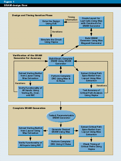
The SRAM was conducted in three phases: design and timing iteration, verification of the SRAM generator, and complete SRAM generation (see Figure 1). The SRAM consists of the array of bits, proprietary circuitry for speed and noise immunity enhancements, decoding logic, and address lines.
Design and timing iteration During the first phase, we created an accurate but compact design of the SRAM. This design is iterated many times for optimization. At the same time, the leaf cells were laid out. Embedded in the leaf cell layout is the information to guide the SRAM generator for assembling the SRAM.
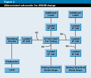
The target goals for the memory were high speed with high noise immunity. To achieve those goals, we embedded proprietary circuitry in the core. Guaranteeing that they were achieved required accurate prediction of the timing, which was done using the abbreviated version of the schematic. The schematic contains a group of bit cells and supporting decoding and sense logic. The aim was to depict accurate loading for a single bit, and model the timing. Achieving the correct timing is a highly iterative process (see Figure 2).
The actual schematic was entered using our graphical tool for entering and managing large IC designs, SUE (Schematic User Environment). At that point, layout data didn't exist, so we entered estimates of the loading into the schematic. The size of the driving circuitry was refined and iterated to achieve the timing goals. We determined and refined the behavior of the bit cell by driving the Hspice simulation from SUE. We modified circuit sizes directly on the schematic and viewed the Hspice output in SUE. The schematic represents the complete logic and circuit model of the final design and is easily modified to simulate SRAMs of different sizes by modifying the loads on the schematic.
SUE has the capability of generating a Verilog netlist automatically from the schematic. At this point in the design flow for more typical designs (random logic or datapaths), SUE would generate the Verilog model for simulation. However, since an SRAM is a large regular structure, it makes more sense to simply build the SRAM and extract the Verilog model from the layout as opposed to creating a large, unreadable schematic.
Because the schematic was small, the iteration time through the analysis tools was quick. Actual sizing and loading information are displayed and attached to the schematic. All circuit simulation data are derived directly from this schematic. A single, compact description is a great aid in design refinement.
To lay out the leaf cells, we used our own tool, MMI Max (abbreviated to Max ). The leaf cells contain information used to overlap, abut, and rotate the cells into place.
The SRAM generator builds a hierarchical structure from the basic leaf cells. The hierarchy of our SRAM is deeper than that of typical SRAMs because of the embedded proprietary circuits. It has seven levels built out of about 50 unique cells.
The generator is an algorithmic description of the construction of the core of the SRAM. It uses the general-purpose megacell generator built on top of Max, which performs the complex data manipulation tasks required to maneuver the cells and add physical features (such as wiring and vias) to the core. This approach keeps the specific SRAM generator to around 200 lines of code.
The generator uses parameters that are directly related to the desired SRAM configuration, such as COLUMNS for the number of columns of SRAM cells, ROWS for the number of rows, and OUTPUTS for the number of outputs. Thus the multiplexing required to get the desired output is simply COLUMNS/OUTPUTS. Different mux-width cells must be laid out and the generator will then select the desired one. Additional parameters describe more subtle characteristics--for example, STRAP_SPACING determines the number of SRAM cells between a well tie, a substrate tie, and a power strap.
The SRAM generator can also algorithmitically add vias to ensure correct decoding of the word lines. This capability is crucial to creating the SRAM generator, because it eases writing a compact, algorithmic description to generate all of the internal connections of the SRAM core, and it keeps the SRAM generator design rule-independent.
At the end of the first phase of the design process, we had an accurate, abbreviated model of the SRAM; the preliminary timing simulation and leaf cell layout have been completed; and an algorithmic description of the SRAM has been construction encoded in the SRAM generator but not verified for accuracy.
Verification of the SRAM generator The goal of the second phase is to verify that the SRAM generator is producing a functionally and physically correct layout. Again, we used a small version of the SRAM so that testing iterations could be performed quickly. At this point, we also refined the full-chip verification techniques so that when the full-size SRAM is generated, the verification methods are known to be good.
We checked the small test SRAM for logical correctness, the critical path extraction for timing verification, and design rule correctness.
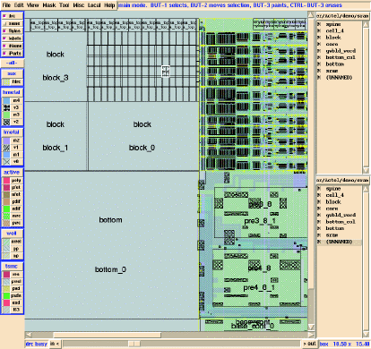
The test SRAM consists of only a few hundred bits and includes a complete set of the decoding and sense circuitry. At least one copy of each cell and all possible layout permutations of each cell are included.
Figure 3 shows a portion of the small SRAM with bounding boxes. The hierarchy has been expanded to several levels in the different cells.
The generator goes through a series of steps to generate the core. First, a 6T cell is placed, a copy is flipped and abutted to the first, and then a copy of both cells is flipped and abutted to the first two. These groups of four cells are placed along a row, and additional cells are spaced within the rows. Rows of 6T cells are built up on each other to a level of four rows deep. An additional row of circuits is added to this structure and the combined structure creates a block. Four blocks are added together to create a larger structure. This structure keeps expanding to produce the required-size SRAM. The generator then creates the spine that connects address lines to memory cells by adding the connections from bit to address line. The vias are added to the address lines by tracing the connectivity from the decoding logic to the cell line and finding where they overlap. At the overlap point, a via is added.
After building the small SRAM, we extracted a Verilog netlist from its layout using Max's extraction capability. Max's extractor builds the Verilog netlist describing the connectivity found in the layout. Max also recognizes the names of the functional cells (such as the 6T bit cell and other custom cells) and substitutes the Verilog description for each cell. The resulting netlist is a complete functional description of the design derived from the layout.
We then run a Verilog simulation with test vectors to verify the netlist. This step guarantees that the megacell generator correctly connected all cells and that there are no inverted signals or other logic problems in the design. The extracted Verilog replaces the schematic for the design. Because the schematic is generated from the layout, the two must match, eliminating the need for LVS.
Testing the small SRAM points out some limitations in the Verilog simulators. Although a reasonable set of test vectors can be simulated with Verilog-XL for the small SRAM, the large SRAM requires too much time and too much memory to perform the same level of verification. On the basis of the small memory, the 256-kbyte SRAM would require hundreds of hours of Verilog-XL simulation and over a gigabyte of real memory.
To address the problem of excessive Verilog simulation time and resource requirements, we developed a compiled cycle-based simulator. NIC converts the Verilog netlist emitted by Max into a functional C program. The tool is capable of converting the switch-level primitives, such as NMOS and PMOS transistors and bidirectional gates. The self-timed design requires three simulation loops for each SRAM access cycle. Even with the multiple-loop evaluation overhead, NIC is two orders of magnitude faster than Verilog-XL. It also greatly reduces the memory necessary to run the simulation--down to a size that easily runs on a 128-Mbyte workstation. With NIC, we can run an extensive verification suite on the full SRAM in a reasonable amount of time using standard workstations.
NIC uses a set of marching addresses and data patterns. Additionally, to compensate for possible bugs in the marching pattern generation, approximately the same number of random address and data patterns are applied. At each clock phase, all outputs are compared with a reference model.
NIC enables us to compile assertions into the simulator. One set of assertion code used is a count of the number of bit cells that are read and written during each clock phase. At the end of each phase, these counters are compared with the expected number of cell reads and writes. Checking the counters ensures that the decoding logic is selecting the correct number of cells each clock phase.
Another assertion ensures the uniqueness of the bit cells. Each bit cell is simulated by several unique lines of code. Each cell's code has a flag for recording the last clock phase that the cell was accessed. If a cell determines it is accessed twice during any single clock phase then it is able to report the error immediately. Comparing the functional simulation with the reference model and checking that the proper number of bit cells are read and written, along with their uniqueness, ensures that the generated SRAM is logically correct.
Mentor Graphics' IC Rules was used to perform DRC on the complete SRAM. By making sure that no DRC violations were created by the generator in the small SRAM, we could be confident that no errors would show up in the larger SRAMs. However, it's always smart to perform a redundant check at such a crucial juncture.
Finally, to extract a Spice netlist of the critical paths from the test memory, we select any cell along a path and click a button in Max to generate the netlist. The Max extractor traces the cone of logic forward to a driving input and then backward to an output, paring all the extraneous logic. Parasitic loads are then extracted and added to the Spice netlist. Then, for the initial design, we simulated those netlists using Hspice. Generating the critical path netlists is done at this point in the design to test the capability of the critical path analysis since the full SRAM hasn't been created yet.
Generating the full SRAM Finally, the actual SRAM is created by algorithmically extending all of the constructs. There is no new layout in the large SRAM, just more of the previous layout. Verifying the full SRAM should now be a single pass, and it was for our first design. Design iterations at this point would be time-consuming and are to be avoided.
Generating a 32-kbyte SRAM takes approximately 15 minutes using a SPARCstation 20 with 64 Mbytes of memory and a 150-MHz processor. Extracting the Verilog netlist from the layout occurs in two steps: resolving terminal names in the hierarchical SRAM in preparation for generating a Verilog netlist and actually extracting the netlist. The whole process takes approximately three hours.
For the full functional simulation of the SRAM, we first use NIC to create a simulation executable. This process takes about four hours and 500 Mbytes of memory and creates an 80-Mbyte executable. The marching and random data patterns are simulated, ensuring the correct functionality of the SRAM. The complete set of patterns on the full SRAM requires about 40 hours of CPU time. By running the executable on several workstations in parallel, we were able to functionally verify the full SRAM in one day. A comparable Verilog simulation would be about 100 times longer and require dozens of 1-Gbyte machines.
To ensure that no errors have been introduced, we run IC Rules on the full design.
Since determining the critical paths in an SRAM is straightforward (the farthest cells from the input), static timing analysis wasn't needed. The final netlist for each critical path contains about 1,500 transistors and takes about 30 minutes to extract from the design's roughly 2 million transistors. We run HSpice on the netlist and compare the timing with the predicted timing from phase one. The compact size of the critical path netlist enables us to perform useful analysis on the layout data.
As a final step, we plot both power and ground and inspect the plots visually. We use Max, which allows nets to be selected and plotted individually. Generating the plots takes a matter of minutes and has proven to be a valuable tool for spotting potential errors.
SRAMs are representative of a class of structures that include other memories and PLDs. We're currently working to extend our methodology to the design of a family of FPGAs. *
Lee Tavrow is the chief engineer at Micro Magic, Inc. (Sunnyvale, Calif.).
John Johnson is MMI's design verification engineer.
Mark Santoro is the president of MMI.
Incorporated in 1995, Micro Magic, Inc. is the industry leader in true 3-dimensional TSV layout tools. Click here for the full story
Engineers from Micro Magic meet with your engineers and management, to discuss the best solution to the problem or problems in the chip design. Some issues are smaller, and more easily remedied; some are larger and will require more involvement. Micro Magic's intention is to provide the most efficient solution utilizing your current design flow and our development tools. Our engineers can either do the work off-site, in house, or provide the MMI tool(s) and advice for a plug-n-play augmentation to your existing flow.
Trying to achieve the performance we needed from commercially-available tools just wasn't working. Over the course of several years, Micro Magic's engineers wound up writing their own tools to help get chips out. Our design services history is unmatched for making tapeout on time. Of course, our clients began to notice that MMI engineers were more efficient, more productive, and started asking about the tools. We responded by making them available to other engineers,and in 1995 the first versions of MAX and SUE were ready for the public..
Micro Magic, Inc.
Sunnyvale, CA
408.414.7647 x202
info at micromagic.com.